
Next-Generation Electronics: Exploring the Role of Metal Stamping in Miniaturization and Component Integration
Next-Generation Electronics: Exploring the Role of Metal Stamping in Miniaturization and Component Integration
Date:2023-12-29 16:33
Introduction
In the ever-evolving world of electronics, the demand for smaller and more powerful devices continues to grow. To meet this demand, manufacturers are turning to innovative technologies like metal stamping to achieve miniaturization and seamless component integration. This article delves into the crucial role of metal stamping in the development of next-generation electronics. By exploring its impact on miniaturization and component integration, we uncover how metal stamping is shaping the future of electronic devices.

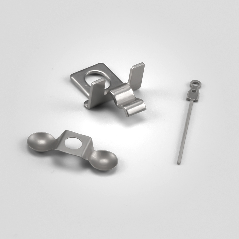
1. Miniaturization: Redefining Size and Performance
Miniaturization is a key driver in advancing electronics, enabling devices to become smaller, lighter, and more portable while maintaining or even enhancing performance. Metal stamping plays a crucial role in achieving miniaturization by allowing the production of intricate and precisely dimensioned components with high accuracy and repeatability. By fabricating miniature yet resilient parts, metal stamping enables the design and manufacture of compact electronic devices without compromising functionality.
2. Component Integration: Seamless and Efficient Solutions
The integration of multiple components within a limited space is a challenge in electronics manufacturing. Metal stamping offers efficient solutions for component integration by producing complex shapes and structures that can be seamlessly integrated into electronic assemblies. With precise tooling and advanced stamping techniques, manufacturers can create custom-designed parts that optimize space utilization, improve connectivity, and enhance overall product performance.
3. Design Flexibility: Enabling Innovation
Metal stamping provides design flexibility, allowing engineers and designers to explore new possibilities in electronic device development. The versatility of metal stamping techniques enables the production of diverse shapes, sizes, and configurations. This flexibility empowers manufacturers to push the boundaries of innovation, creating novel designs to meet evolving market demands. From intricate connectors and microelectromechanical systems (MEMS) to high-density interconnects metal stamping facilitates the realization of cutting-edge electronic device designs.
4. Enhanced Reliability and Durability
Reliability and durability are essential attributes of any electronic device. Metal stamping ensures the production of robust components with high structural integrity. By leveraging advanced materials and precise manufacturing processes, metal-stamped parts exhibit superior mechanical strength, resistance to environmental factors, and prolonged lifespan. This enhances the overall reliability and durability of electronic devices, decreasing the risk of failure or malfunction.
5. Streamlined Production Processes
Metal stamping offers streamlined production processes that improve efficiency and reduce costs in electronics manufacturing. Through automation and high-speed stamping lines, manufacturers can achieve higher production volumes while maintaining consistent quality control. The repeatability and accuracy of metal stamping processes enable rapid and cost-effective mass production of electronic components, meeting the demands of a competitive market.
6. Sustainable Manufacturing Practices
Sustainability is gaining prominence in every industry, including electronics. Metal stamping aligns with sustainable manufacturing practices by optimizing material usage and reducing waste generation. With efficient production techniques and recyclable materials, stamped components contribute to a more environmentally friendly approach to electronics manufacturing. Furthermore, the longevity and reliability of metal-stamped parts promote product sustainability by reducing the need for frequent replacements.
7. Collaboration Fuels Technological Advancements
Collaboration between metal stamping experts, electronic design engineers, and research institutions drives technological advancements in the field. By sharing knowledge and expertise, these collaborations lead to the development of improved stamping techniques, materials innovation, and process optimization. Continued collaboration fosters ongoing progress in metal stamping technologies, contributing to further miniaturization, enhanced component integration, and the realization of next-generation electronic devices.
Conclusion
Metal stamping plays a pivotal role in shaping the future of electronics by enabling miniaturization, seamless component integration, and design flexibility. From compact devices to complex electronic assemblies, metal stamping empowers manufacturers to create smaller, more powerful, and technologically advanced products. With its emphasis on reliability, streamlined production processes, sustainability, and collaborative innovation, metal stamping is at the forefront of next-generation electronics manufacturing. As technology continues to advance, metal stamping will remain a vital tool in driving the evolution of electronics and meeting the demands of an increasingly connected world.
Share to:
Recommend wonderful blog posts